Chinese English
Contact
  • Telephone
    135-5591-3966
  • Fax
    0411-65835291
  • Website
    www.anciento.com.cn
  • Address
    Room 901, Kechuang Building, 131 Guangxian Road, Dalian High-tech Park
Optical curvity / surface profile
Position: Home > Product > Optical curvity / surface profile
Flatness Detector
Non-contact wafer flatness measurement, TTV, bow, warp and flatness/warpage measurement
It is suitable for the detection of transparent crystal objects (such as sapphire wafers) and LED epitaxy wafers and chips.
It is suitable for measuring instruments of various wafer sizes and materials.
Overview:
Product series models include manual and fully automatic modes.
It can measure almost all materials including Si, GaAs, InP, Ge, etc.
Powerful software functions can test the flatness of TTV, bow and war in a few seconds.
In addition, the stress of the wafer before and after processing can be calculated by measuring the same wafer twice before and after processing.
All calculations are in accordance with ASTM and Emi standards to ensure compatibility and uniformity with other process instruments.
Characteristic:
Measurable wafers (silicon, glass, etc.)
The company's unique graphics and image analysis method provides data storage and analysis functions, and can output detection reports.
The device has barcode or two-dimensional code reading function, and can calculate the stress changes caused by warpage.
Provide automatic interface to realize on-line automatic detection
The repetition accuracy is 0.3 micron and the detection speed is fast (up to 15s per piece).
Technical index:

一、 Software Operating Interface

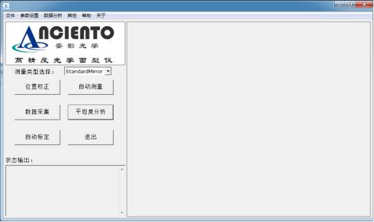
Main Operation Interface:

Flatness Analysis Interface:

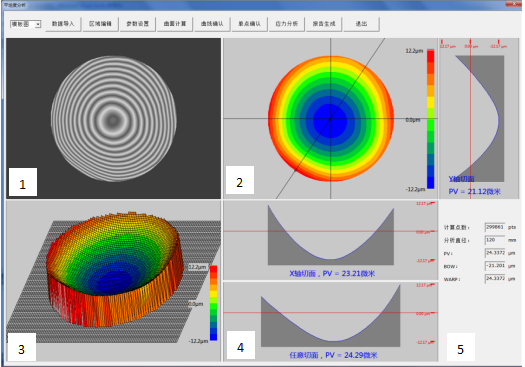
1 is fringe analysis, 2 is surface analysis, 3 is sample three-dimensional analysis, 4 is arbitrary section analysis, 5 is analysis data.


Stress Analysis Interface:

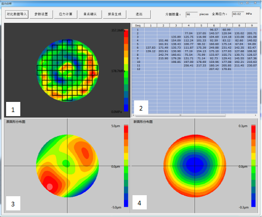
1 is stress analysis diagram, 2 is stress diagram of cutting unit, 3 is stress front diagram, 4 is stress analysis diagram.

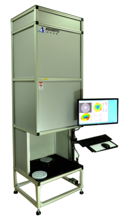
二、 Hardware Selection